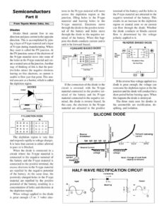
Semiconductors Part Il From Toyota Motor Sales, Inc. Diodes Diodes block current flow in one direction and pass current in the opposite direction. This is accomplished by join- ing a layer of P-type material and a layer of N-type during manufacturing. Where they meet is called the PN junction. At the PN junction, some of the electrons of the N-type material move into some of the holes in the P-type material and cre- ate a neutral area at the junction. Another way of thinking of this is that the posi- tive holes attract the negative electrons leaving no free electrons, so current is unable to flow past that point. This neu- tral area acts as a barrier, which is called the depletion region. DIODES Symbol Anode Cathode Actual diode P N JUNCTION DIODE N The depletion region is very thin and responds rapidly to voltage changes. It is here that current is either allowed to pass or is blocked. When the diode is connected in a circuit where the N-type material is connected to the negative terminal of the battery and the P-type material is connected to the positive terminal, the excess electrons in the N-type material are repelled by the negative potential of the battery. At the same time, the positively charged holes in the P-type material are repelled by the positive potential of the battery, resulting in a concentration of holes and electrons at the depletion region. When voltage applied to the diode is great enough (.5 to .7 volts) elec- trons in the N-type material will move across the depletion region at the junction, filling holes in the P-type material and leaving holes in the N-type material. Electrons move through the diode to the positive termi- nal of the battery and holes move through the diode to the negative ter- minal of the battery. When this hap- pens the diode conducts current and is said to be forward biased. FORWARD BIASED DIODE P ®@ ® ®@ Or Electron flow Conventionat current flow Hole flow } = @'”‘S If the connection of the diode in the circuit is reversed, with the N-type material connected to the positive ter- minal of the battery and the P-type material connected to the negative ter- minal, the diode is reverse biased. In this case, the electrons in the N-type material are attracted to the positive terminal of the battery and the holes in the P-type material are attracted to the negative terminal of the battery. This results in an increase in the depletion region or neutral zone so no current can flow through the diode. Whether the diode conducts or blocks current flow is determined by the voltage polarity applied to it. REVERSE BIASED DIODE No electron flow No hole flow If the reverse bias voltage applied to a diode is great enough, the voltage can overcome the depletion region at the the junction and the diode will conduct for a short period before burning open. When this happens the diode is destroyed. The three main uses for diodes in the automobile are rectification, de- spiking, and isolation. Reverse Reverse Current Sewanee named Reverse bias voltage Avalanche current , 7 ( smokes? war SILICONE DIODE Forward current breakdown 500 400 300 200 100 {mA} Reverse current Forward operating current (mA]} a Forward bias voltage Note: Change of scale from reverse ta forward HALF-WAVE RECTIFICATION CIRCUIT Conducting Input Blocking